The IC industry is always challenging for thinner packages with smaller footprint. Though the flip-chip technology has various advantages over the other high-density electronic packaging approaches, there are rising challenges to ensure moldability and minimize defects with rapid advances in flip chip technology such as decreasing bump pitch, stand-off height, thinner package profiles and molded materials.
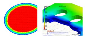
During the fabrication of epoxy molding compound in IC encapsulation process, stress-induced problems such as wire sweep and paddle shift are the most common problems. The viscous drag force on wires exerted by the resin melt flow causes wire sweep, while non-uniform force loading on paddle results in paddle shift.
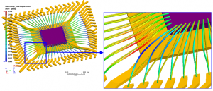
In figure, the position of wire cross over is shown in a closer look. In the wire crossover display, the shape of wires are shown as deformed mesh on true scale, and wires contact each other will be marked in red, while other wires remain theirs original color.
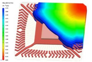
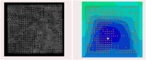
During the post mold cure process, the volume of EMC will shrink due to the effect of cross-linking and undergo the stress relaxation due to viscoelastic behavior. In addition, because of the fact that the coefficient of thermal expansion of each element in the encapsulated unit is different, a warpage issue will have a high probability to occur in this process as well. If the warpage problem is too severe, the internal microstructure of the encapsulated unit might be damaged, cracked, or malfunctioned.
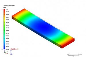
The Z-displacement when the IC unit is removed from the oven to room temperature at the end of the post-mold cure process. The simulation of the final warpage is 0.354 mm, which is very close to the experiment result.